Bruker NanoWizard 4 XP Nanoscience AFM
Bruker NanoWizard 4 XP Nanoscience AFM
Extreme performance meets utmost flexibility

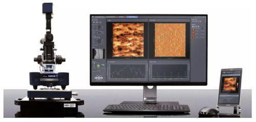
The NanoWizard® 4 XP NanoScience atomic force microscope delivers atomic resolution and a large scan range of 100 µm in one system. It enables fast scanning with rates of up to 150 lines/sec and seamless integration with advanced optical techniques. A wide range of modes and accessories for environmental control, mapping of nanomechanical, electrical, magnetic or thermal properties, makes it the most flexible system available on the market today.
Features:
- PeakForce Tapping® for easy imaging
- Fast Scanning option with up to 150 lines/sec
- NestedScanner Technology for high-speed imaging of surface structures up to 16.5µm with outstanding resolution and stability
- New tiling functionality for automated mapping of large sample areas
- V7 Software with revolutionary new workflow-based user interface
- DirectOverlay™ 2 software for perfect integration and data correlation with advanced fluorescence microscopy platforms
- Vortis™ 2 controller for high-speed signal processing and lowest noise levels
Automated analysis of large sample areas with new tiling functionality
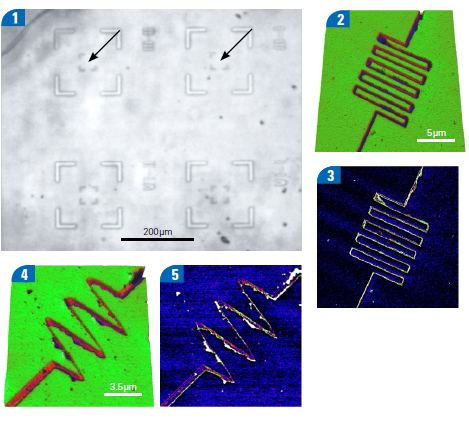 The fastest and easiest way to navigate is to see where you want to go. DirectOverlay 2 provides instant navigation, with direct selection of measurement positions anywhere within the scanner range. The Motorised Precision Stage and HybridStage™ free experiments of the lateral constraints of the AFM piezo range, and allow direct motorised movement to selected positions.
The new DirectTiling feature automatically creates a large optical overview to accelerate this process. Multiscan enables tiling of high-resolution images to build up a comprehensive overview of the sample. Repetitive or complicated measurement sequences can be automated using ExperimentPlanner™ macros.
The images show PDMS stamped surface pattern, sample courtesy of Dr. Claudio Canale, University of Genoa, Italy. [1] Optical image of reference pattern. Four square regions are marked with a concentric corner pattern, the inner corners form a 50 micron square with test patterns printed in the center, but not visible in the optics. Imported into the SPM software with DirectOverlay, such images allow single-click navigation between reference positions separated by many times the piezo range. QI Advanced images of two such reference patterns (see arrows), topography [2] + [4] and adhesion images [3]+ [5].
For further information please contact us or download the datasheet.
