Webinars

Webinar : Compact and Upgradeable Benchtop Fluorescence Microscope
Date : Wednesday 27 November 2024
Time : 5am NZDT, 3am AEDT, Midnight AWST
Speaker : Dr Geraint Wilde
If you are not a night owl, please register and a recording will be emailed to you

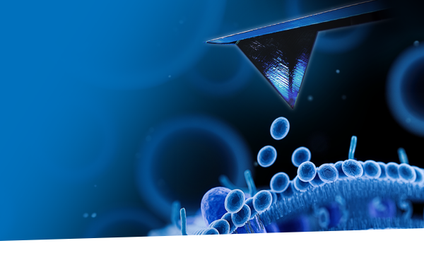
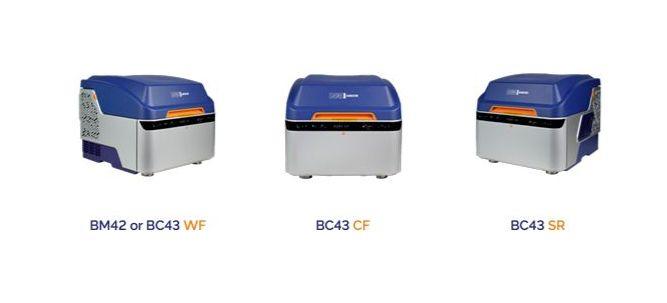
Andor is excited to announce the expansion of our Benchtop Microscope range, adding application and budget-based flexibility to the original BC43 Benchtop Confocal. Their Benchtop Microscopes now start with motorised multi-dimensional widefield fluorescence imaging and extend into super-resolution range.
They will introduce the new products and the different imaging modalities of widefield, confocal and super-resolution fluorescence microscopy. The biological models and typical experiments those modalities can be optimally used with will be discussed.
Being a modular design, they will cover how our latest products can be upgraded in the field over time as your research needs change.
Learning Objectives
- Learn about the new extended BC43 product range
- Gain Insight into different imaging modes (widefield, confocal and super-resolution) and the sample types they are applicable to
- Understanding the achievable multiple scales of imaging
Read More
Webinar : Performing Accurate Force Measurements on Biological and Soft Matter
![]() Date: Wednesday 23 October
Date: Wednesday 23 October
Time: 2am AEDT, 4am NZDT, 11pm AWST

Join us and special guest speaker Prof. Andreas Janshoff from Georg-August University Göttingen, Germany, for this webinar on performing accurate force measurements on biological and soft matter using atomic force microscopy (AFM).
Forces play a crucial role in biological mechanisms, such as cellular response, molecular interactions, and protein binding, and are essential for deriving the nanomechanical properties of a sample. AFM has emerged as a key platform for the precise measurement of interaction forces on the nanometer scale. AFM force spectroscopy is used to quantify forces and determine nanomechanical properties such as Young's modulus, cell adhesion, and viscoelastic properties, information that is invaluable for studying interaction-based and disease-related biomechanical changes.
Prof. Janshoff will outline his work using AFM to investigate the biomechanical properties of cell membranes, and, in particular, the viscoelastic behavior of the cell cortex.
Webinar Highlights:
- Key insights and proven strategies for achieving reliable results
- Common pitfalls and practical tips for ensuring reproducible measurements
- Q&A session with the team
Webinar : Introducing Bruker's Next Gen Stylus Profilometer
![]() When : Tuesday 29 October 2024
When : Tuesday 29 October 2024
Time : 7pm NZDT, 5pm AEDT, 2pm AWST

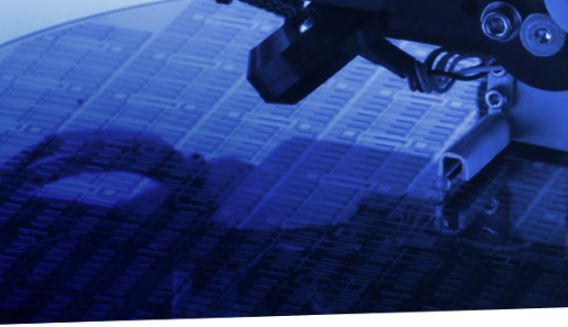
We will introduce Bruker’s new 11th generation Dektak Pro Stylus Profiler, providing even more enhanced operability, reliability, and measurement accuracy to enhance and extend the qualities that make Dektak synonymous with stylus profiling.
Additionally we will explore how stylus profilers can characterise a diverse range of materials, particularly in microelectronics and semiconductor applications. Many processes in semiconductors, optical coatings, and micro-electromechanical systems (MEMS), as well as research in flexible electronics and sensors, depend on accurate thickness and etch-depth measurements. Among their various metrology capabilities, stylus profilers excel at delivering exceptional step height measurements at both the nanoscale and microscale.
Read More
Compact and Upgradeable Benchtop Fluorescence Microscope
Date: Wednesday 19 June 2024
Time: 3am NZST, 1am AEST, 11am AWST
If you are not a night owl register for the webinar and you will receive a copy after the event :)
With the latest expansion of our Benchtop Microscope range, adding application and budget-based flexibility to the original BC43 Benchtop Confocal. We can now offer more choice and scales of imaging for Neuroscience studies. Our Benchtop Microscopes now start with motorised multi-dimensional widefield fluorescence imaging and extend into super-resolution range.
We will introduce our new products and the different imaging modalities of widefield, confocal and super-resolution fluorescence microscopy. The typical biological models and experiments those modalities can be optimally used with will be discussed.
Learning Objectives
- Learn about the new extended BC43 product range
- Insight into different imaging modes (widefield, confocal and super-resolution) and how they can be applied to typical neuroscience research models and experiments.
- Understanding the achievable multiple scales of imaging.
Geraint Wilde attained a Ph.D. in Neuroscience in 1997 from the University of Southampton, UK, and then continued in the field with a postdoctoral position at the University of Warwick, UK. Having developed an interest in microscopy during his Ph.D. and post doc, he moved to the University of Liverpool, UK, to work in the laboratory of Michael White, focusing on intracellular signalling and gene expression through live-cell imaging. Geraint then left academia to pursue a commercial career in microscopy, starting as a Sales Application Specialist for general life science microscopy where he was exposed to an even broader range of microscope technology and most importantly applications. He joined Andor Technology in 2009, where he is now Hardware Business Manager for Microscopy and Life Science Cameras and the Product Manager for the Andor Benchtop Microscopes.
Read More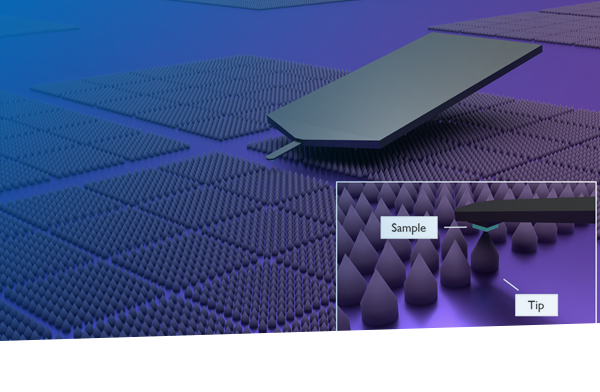
Reverse Tip Sample (RTS) Scanning Probe Microscopy
 Date: Wednesday 19 June 2024
Time: 3am NZST, 1am AEST, 11am AWST
If you are not a night owl register for the webinar and you will receive a copy after the event :)
Our guest speakers for this webinar developed Reverse Tip Sample (RTS) Scanning Probe Microscopy (SPM) to overcome the single-tip barrier of traditional SPM. By placing the sample on a tipless cantilever and the tip on the sample stage, RTS SPM essentially flips the conventional tip-sample positions.
The standout feature of this arrangement is the ability to change tips seamlessly, greatly boosting data collection efficiency in application spaces requiring frequent tip replacements. During operations in RTS configuration, the cantilever-mounted sample scans one of thousands of tips present on the probe chip. When a tip wears out, the operator repositions the cantilever onto an adjacent fresh tip, which takes mere seconds.
After a comprehensive introduction of the RTS SPM concept, this webinar will further discuss:
- Nanofabrication of probe chips and a dry etching process for fabricating high-quality Si probe chips, which features a novel tip sharpening step. The application of metal and diamond coatings on these Si probe chips will also be covered.
- Sample preparation, including dependable workflows developed for routinely preparing RTS SPM samples by focused ion beam (FIB) and FIB-less approaches. These time-efficient procedures yield RTS samples with excellent electrical contacts and mechanical stability.
- Measurements and applications of RTS SPM, such as statistical multi-tip studies, RTS Scalpel SPM, electrical tomography, and more.
Webinar Speakers:
Nemanja Peric, Ph.D., SPM Researcher, imec, Belgium
Pieter Lagrain, Engineer, imec, Belgium
Peter De Wolf, Ph.D., Senior Directory Technology & Application Development AFM, Bruker
